Wednesday, December 23, 2009

Latest news: new picosecond accelerator operational - 23th of December 2009

Our new picosecond pulsed high-energy electron accelerator has delivered its first pulses today (23 December 2009). Pulses are being produced for pump and probe experiments with a world-wide unprecedented high repetition frequency of 100 Hz.

This terrific achievement is the outcome of intense collaboration and commitment of technicians and scientists at the Department of Chemical Engineering and the Reactor Institute Delft.

In particular Martien Vermeulen and Walter Knulst have shown enormous persistence since they started the design and construction of the accelerator about four years ago.

The electron pulses will be combined with optical and terahertz probe pulses for studies on new materials for application in opto-electronics (e.g. solar cells) and nanomedicine.


Movie of the electron beam - 23rd of December 2009


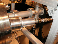
1 - The Sample Chamber has an extra port through which we can see the sample in the Sample Chamber from the front side. This makes is possible to place a CCD Camera behind this window and monitor the beam position and shape by using a phorphor screen at the sample position.


2 - The CCD image. In the center you can see the phosphor screen positioned in the center of the Sample Chamber.


Here you can see the movie with the electron beam visible on the phospor screen.

UV generated electron pulse - 23rd of December 2009

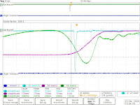
A view scope images. In purple the forward RF pulse, in green the reflected RF pulse, in light blue the beam dump signal measured over 50 Ohm.


1 - Clearly visible the large light blue spike which is the UV generated electron pulse measured in the beam dump.


2 - Same situation only now with the background of dark current visible. This can be achieved by changing the strength of the main magnet around the cavity.


3 - Now, we made the RF pulse shorter and changed the timing of the laser so that it arives at the end the RF pulse when the electric field in the cavity reaches it maximum.


4 - Zoom in at the end of RF pulse.

The Great Day - 23rd of December 2009

On the 23rd of December we prepared the UV laser beam and synchronization to excite the first electron pulses.


Walter Knulst and Martien Vermeulen who have contructed the picosecond-pulsed 4.5-MeV electron accelerator. This project could not have been successfull without the support and help of many people: John Suijkerbuijk, Paul Rijkers, Juleon Schins, Laurens Siebbeles, Rene den Oudsten, Raymon Bresser, Rene Gommers, Ruud van Tol, Eindhoven University of Technology, Pulsar Physics, and many others.


2 - On the scope screen in blue the UV excited electron pulse is visible. To celebrate this event a bottle of champagne is donated by Laurens Siebbeles, the initiator of the accelerator project.


3 - We invited a lot of contribitors to the construction of the electron accerlator to see the first electron pulses on screen and take part of the celibration.


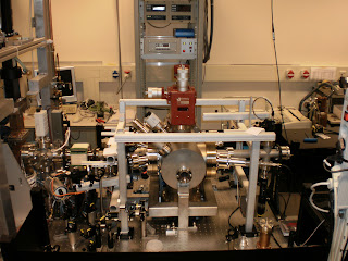
4 - Taking a look at the setup.

5 - Taking a view at the setup.

Wednesday, December 2, 2009

Synchronization of laser system with accelerator - December 2009

In this post, I will present some details about the synchronization of the laser system with the RF electron accelerator.


1 - A photodiode monitors the 75-MHz output of the Ti:S oscillator. This signal is transported to a Phase Lock Loop than synchronizes a 3-GHz Voltage Controlled Oscillator to this laser, with ability to control the phase. This system has been published by Kiewiet et al. in 2001. The laser oscillator is the main clock of the system. To match the derived 3-GHz frequency to the resonance frequency of the RF cavity, the laser cavity length can be changed by displacing one of the end mirrors.


2 - These two boxes allow us to trigger the laser system by one external trigger from the main Trigger and Delay Generator. One trigger to the laser system leads to a pulse from the high power pump laser of the amplifier and the pulse selection by the two Pockel Cells in the regenerative amplifier cavity. This system operates at 1-kHz frequency.


3 - Because the accelerator operates at 100-Hz or lower frequency the laser frequency is down shifted by the use of a chopper and shutter combination. The chopper decreases the frequency to 100-Hz from which a fast shutter can select only a single pulse or it sub harmonic. We perform this operation to prevent the cathode of the RF cavity of being exposed to too many laser pulses that can cause damage.


6 - In front you can see the shutter and in the back the vacuum laser transport line to the accelerator room.


7 - The chopper and shutter controllers. The chopper is synchronized to the 1-kHz trigger of the laser system. Then only the right phase has to be selected to pass the right laser pulse from the 1-kHz train.

Details of Laser Beam - December 2009

In this post, I will present some details of the optical layout.


1 - This is the side optical table. In the right corner in the front the laser beam transport line can be seen. Through this vacuum line the 800-nm fundamental laser beam from the Ti:S amplifier is transported. Using vacuum reduces instabilities in the laser beam caused by turbulence of air flow.


2 - We choose to transport the stretched amplified laser pulse directly output of the regenerative amplifier. At the output of the laser system a telescope is positioned to shape the laser beam to a smaller size. On this picture you see the compressor that is positioned on the side table.


3 - After the compressor the laser beam passes through the second and third harmonic unit. The third harmonic is used either to generate the electron pulse at the cathode surface of the RF cavity or excite the sample optically. The left over fundamental beam will be used to probe the sample. If necessary this fundamental wavelength can be converted into other wavelengths by using for instance white light generation.


4 - Around the Sample Chamber a frame is mounted to hold the opto-mechanical components. The laser beams (pump and probe) have to be deflected upwards to reach the windows of the vacuum system.


5 - Detail of the UV in coupling. One can see the prism's in the cross.


6 - Detail of the probe laser beam transport line to the window of the Sample Chamber.

Tuesday, December 1, 2009

Details of Sample Chamber - December 2009

In this post, I will introduce some details of the Sample Chamber and explain their function.


1 - At the side of the Sample Chamber one can view through a big window into the chamber and see the carousel holding multiple samples. We have a standard piece mounted with diaphragm’s, a phosphor screen and test samples such as ZnS and ZnSe.


2 - The rotational feed through mounted on a x,y,z stage. We can rotate the right sample into the electron beam, retract the complete carousel out of the electron beam line and displace the sample through the electron beam.


3 - Behind the sample chamber but before the electron beam dump a beam viewer can be inserted into the electron beam. Using a Gigabit Ethernet CCD Camera we are able to follow the electron beam at a high frame rate.


4 - Here you see the beam dump at the deflected output port of the sample chamber. Using this beam dump, we can optimize the electron beam without irradiating the sample and causing unwanted degradation.


5 - Input window of the laser beam to the sample. We are not only able to excite the samples with the electron pulses, but in the same sample chamber we can excite them also with the laser pulse. In this way we can compare laser flash photolysis with electron beam photolysis without exchanging the sample to different experimental setups.

Monday, November 30, 2009

Details of Electron Beamline - December 2009

In this post I will introduce the components of the beamline and explain their function.

1- Directly behind the RF cavity and RF input coupler a valve is positioned to separate the vacuum compartment of the cavity from the rest of the setup.


2- Then around the bellows a steering magnet is positioned. With this magnet we are able to position the electron beam on the sample and find the overlap with the probe beam. The probe beam is a time delayed ultrashort laser pulse than analyses the status of the sample after being excited by the electron pulse.


Additionally, we are able to displace the electron beam over the full sample surface. This is necessary, because the electron pulse is causing irreversible damage to the sample. By taking each time a fresh piece of sample, the measurement time can be extended before replacing the sample.

3 - Next, we have a cross-piece which is used to couple the UV pulse into the vacuum system to illuminate the cathode surface and generate the electron pulse. We use 266-nm laser light, which is the third harmonic of the 800-nm fundamental wavelength coming from a Ti:S amplifier.

In this cross-piece two aluminum coated prim's are mounted on a moving base. This base is constructed in such a way that when rotating the feed through below the gap between the prima's can be varied. One has to realize that the UV beam has to pass through the inner conductor in the coaxline upstream to the cavity. This has a narrow diameter. On the other hand, the prism's have to be placed to the side, because the electron beam is passing through the center. Due to the control of the gap, we can find the optimum position of the prisma's. Finally, the reflection of the UV pulse on the cathode surface can be seen at the output window. This is essential to find with the UV laser beam the center of the cathode surface. One can see all the diamond turning rings in the reflection of the UV laser beam.


 4 - Sample chamber. It is a very complex piece. The essential function is that a carousel with multiple samples can be positioned with respect to the electron beam using a rotational feed through with x,y,z linear stages. The chamber has four laser windows (two input and two output) mounted at small angles with respect to the electron beam to probe the sample. We like to setup a visible probe line and a infrared probe line.
5 -In front of the sample chamber a bending magnet is mounted. This enables us to deflect the beam away from the sample into a side beam dump. This function serves multiple purposes: We can scan the electron beam energy; We can optimize the phase injection of the UV laser beam into the RF cavity; We can measure the background level to correct the measurement; By rapid switching of this magnet we prevent the sample from degrading and exposure to excessive electron pulses.

Saturday, November 28, 2009

Installation of beamline including the Sample Chamber - December 2009

In a previous post, I have introduced the concept of the beamline and Sample Chamber. Due to the failure of the orginal RF Window, the accelerator was out of order for at least two month. Due to this long break, we decided to upgrade the beamline and started to install the Sample Chamber into the beamline.

Below, you will find some pictures of the Sample Chamber. Beginning of December the complete chamber was installed.


Sample Chamber after the vacuum beaking out procedure.


Viewed from the other side. In the slot of the optical table you can see a large valve in the connection piece to the turbo pump.


Sample Chamber installed on the optical table. The RF cavity is situated at the left side.

Wednesday, September 30, 2009

RF Window problems - September 2009

Shortly after we have achieved very good RF processing results in September 2009, we had a serious RF breakdown event at the RF window. This RF window separates the RF waveguide section at SF6 overpressure from the RF cavity at high vacuum.

In short, while running the klystron at about 7.5 MW output power a breakdown event occurred at the vacuum site of the RF window. We installed photodiodes to monitor breakdown light flashes from the RF cavity and from the RF window. At this specific event the light output from the window was evident. After this event, we had to turn the RF power level down to 1 MW and even then small discharges were appearing each pulse. RF processing did not improve this situation and lead to the conclusion that the RF window has been damages and had to be replaced.

We decided to replace the current CPI RF window of type VWX-1053 with a pillbox type RF window. After consulting some manufactures, we have ordered a RF window from CML Engineering of type 3020-02. This window has higher specifications in terms of peak and average RF power level and therefore will be more reliable. At the end of November 2009 this RF Window and adapter piece has been delivered.

The RF window that was installed originally.


The new RF window of CML Engineering
installed in the RF section. The connection
at the bottom is to the adapter piece for
the connection to the RF input coupler of
the RF cavity.

Side view of the RF window.

Thursday, September 17, 2009

Milestones achieved during RF processing - 10th of September 2009

While continuing RF processing of the RF cavity, the level of RF input power is gradually increasing. For instance, on the 10th of September we could ramp up very fast up to 3.9-MW input power and 3.0-MeV electron energy at 50 Hz without experiencing any breakdown.

By the end of the day the level of 7.1-MW input power and 3.8-MeV electron energy has been reached in case of a 1.0-us short pulse and 40-Hz repetition frequency. The measured peak dark current was 0.17 mA and the charge per pulse was 0.079 nC.


7.0 MW and 3.8 MeV


7.1 MW and 3.8 MeV

First accelerated electrons - 3th of September 2009

During the first week of September we continued the RF processing of the RF cavity.

The second day we also turned on the main solenoid magnet around the RF cavity. As a result we had to repeat the training session of the day before, because the magnet influences all the processes inside the cavity. For instance, field emitted electrons follow different paths when the magnet is turned on.

On the 2nd of September we soon reached 3.0-MW input power and 2.4-MeV electron energy. We continued the RF processing by replacing the 10-dB attenuator at the input of the preamplifier to 6 dB. Now we sometimes observe breakdown events with a measurable electron signal on the beam dump at the exit of the cavity and at the same time observe a light pulse on the photodiode that looks inside the RF cavity. Surprisingly, not all breakdown events are accompanied by electrons and light. Possibly, these events are taking place outside the RF cavity. By the end of this day, we have reached 3.6-MW input power and 2.9-MeV electron energy operating at 50 Hz.

The 3th of September was a very exciting day, because we observed for the first time dark current coming out the RF cavity. The power level at that moment was 3.7-MW input power and 3.0-MeV electron energy. We were able to optimize the setting of the main solenoid magnet around the cavity by maximizing the dark current on the beam dump. We also observed single-side electron multipacting at the photocathode in the RF gun (see Han et al. in Phys. Rev. ST AB 11, 013501 (2008)). For instance, we have measured at the setting of 3.9-MW input power and 3.0-MeV electron energy a peak dark current of 52 nA and a total charge of 0.11 nC per pulse.

Below you can find two oscilloscope images displaying with the following signals: Light Blue - Modulator current; Purple - Forward RF Pulse; Green - Backward RF pulse; Dark Blue - Beam dump signal.


The first observation of dark current out of the RF cavity measured at the beam dump at the exit.


Dark current at a higher setting of the acceleration field.

Wednesday, September 16, 2009

FIrst RF Processing session of RF cavity - 31th of August 2009

On Monday 31th of August 2009 it was the day of starting the RF Processing procedure.

RF Processing is a neccesary step during the installation of the RF accelerator in which gradually increased RF power is applied to the cavity in order to clean and smoothen the inner surface. As a result the cavity can hold increasingly higher electric field levels without resulting in a breakdown event.

In order to perform a successful RF processing procedure, we have equiped the setup with several detection systems:
1- Breakdown detector: A piece of analog electronics monitors the backward reflected RF waves from the cavity and senses very abrupt changes in RF power that will occur upon breakdown inside the cavity. This is due to the change of impedance of the cavity when a breakdown occurs. When a breakdown is detected the RF pulse is immediantely interrupted.
2- Vacuum pressure monitor with switch: When the vacuum pressure inside the cavity exceeds a certain level the RF power to the cavity will be interupted untill the pressure has droped below the level again.
3- Faraday cup or electron beam dump at the exit of the cavity to monitor the electrons coming out of the cavity. The signal is presented on an oscilloscope.
4- Photodiode that monitors the light output of the cavity to detect the intensity of the breakdown event. The signal is presented on an oscilloscope.
5- Photodiode that monitors the light output near the RF window to detect the intensity of the breakdown event.

We have a few parameters that we can set in the system:
1- RF peak power by changing the RF input power to the Klystron tube by changing a variable discrete attenuator between 0.0 and 15.5 dB in steps of 0.5 dB.
2- RF peak power by changing the high voltage setting of the modulator. This can be seen as a fine adjustment of the RF power as compared to option 1.
3- RF pulse length by changing the modulator pulse length. This can be changed between 0.50 and 2.80 us flat top.
4- RF pulse repetition frequency can be set between 0 - 100 Hz as long as the average power of the modulator does not exceeds 6.5 kW. In general, we do not exceed 50 Hz.

The method that we apply is to start with the setting of the shortest pulse and increase in RF power. After a certain level has been achieved, the pulse length is increased, while keeping the maximum field strength in the cavity constant. Do to this the RF filling time of the cavity has to be taken into account. Once dark current is observed from the cavity, this is easily achieved by keeping the dark current constant. The last step is to increase the pulse repetition frequency. This procedure can be repeated untill the maximum RF input power is reached.

At 18:00 that day we started under supervison of the radiation safety department of TU Delft the RF processing procedure. We replaced the 20 dB attentuator at the input of the preamplifier to a 10 dB. Soon after the start we reached the level of 1 MeV electron energy. By midnight we haved reached 2.9 MW input power and 2.5 MeV electron energy. The estimated electric field inside the cavity is about 60 MV/m.


The accelerator is control from the control room. Left to right: Juleon Schins, Laurens Siebbeles, Koos van Kammen and Walter Knulst.


Walter Knulst is controling RF processing from the accelerator GUI build in LabView.


Walter Knulst together with Martien Vermeulen who is the allround electron accelerator engineer.


Another look at the control room.


A breakdown event is recorded by the oscilloscoop. In green you can see the abrupt change in RF reflection from the cavity and 400 ns later the breakdown detector has switched of the RF power.


Another breakdown event, which has unfortunately not been detected by the breakdown detector due to the fact that the rising edge is less steap than the event to the left.